Pin Properties
pin properties
The pins of a schematic symbol are one of the most important parts of a component, allowing wire connections to be made to make up an entire circuit.
Top Toolbar - Place - Pin or use shortcut "Ait + P

Pin orientation
Before placing on the canvas, you can press the space bar to select to the desired direction. The circled end of the pin is where a wire connection can be made, so this point should normally be placed outwards.
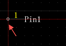
correct format
pin properties
When you select a pin, you can view and modify its properties in the properties panel on the right.
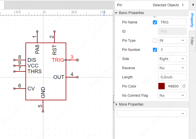
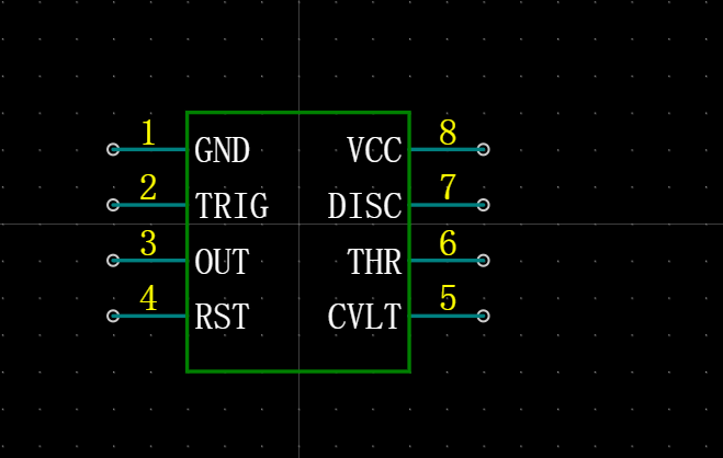
Name: The name of the pin, as shown in the above figure, the name of the selected pin is "VCC".
ID: The ID of the pin is fixed by the system and cannot be changed.
Type: selectable input, output and bidirectional.
Pin Number: The pin number selected as above is "8". **The number corresponds to the pad number of the footprint corresponding to the component, and the numbers of the two need to be consistent. **You can also use numbers with letters, such as A1, B1, C1, A2, B2, etc.
Pin Direction: Only supports up, down, left, and right directions, other directions are not supported for the time being.
- NON-PIN: Whether it is a pin selection.
Length: Pin length.
Pin Color: You can modify the color of the pins.
Added attributes: EasyEDA Pro can customize the added attributes.