EasyEDA Pro Quick Start
EasyEDA is a browser-based, user-friendly, powerful EDA (Electronics Design Automation) tool. It was founded in 2010 and is now an important department of JLC Group. EasyEDA serves a large number of electronic engineers, educators, students, enthusiasts and electronic design companies. It is committed to the one-stop experience of schematics, circuit diagram drawing, simulation, PCB design and manufacturing of small and medium-sized circuits (about 10,000 pins).
EasyEDA has the following features:
- Lightweight: EasyEDA does not require the installation of any software or plug-ins. Just open the browser to use it, or download the client to support offline use. The recommended browsers are Google Chrome, Edge browser and Firefox browser.
- High performance: The same operating efficiency and speed as traditional mainstream EDA tools can be achieved in the browser. Some performance is even better.
- Years of accumulation: EasyEDA is the domestic version of the well-known online EDA software EasyEDA. EasyEDA focuses on domestic users, while EasyEDA focuses on foreign users.
- Cross-platform: Whether you use Linux, Mac, Windows, or anywhere you use it, visit the address: https://pro.easyeda.com/editor
- Independent and controllable: completely independently developed by Chinese people, with independent intellectual property rights.
- Good support: Domestic users provide friendly community support. For the community, please visit: https://oshwlab.com/forum
- Rapid updates: actively respond to user needs, update quickly, and meet different user needs.
- Special features: It has innovative special features, which is more in line with the usage habits of Chinese people and improves work efficiency.
This chapter will introduce you how to use EasyEDA Professional Edition in a simple, fast, and full process to complete a quick start. Achieve two hours of getting started and three days of mastery.
Install the client
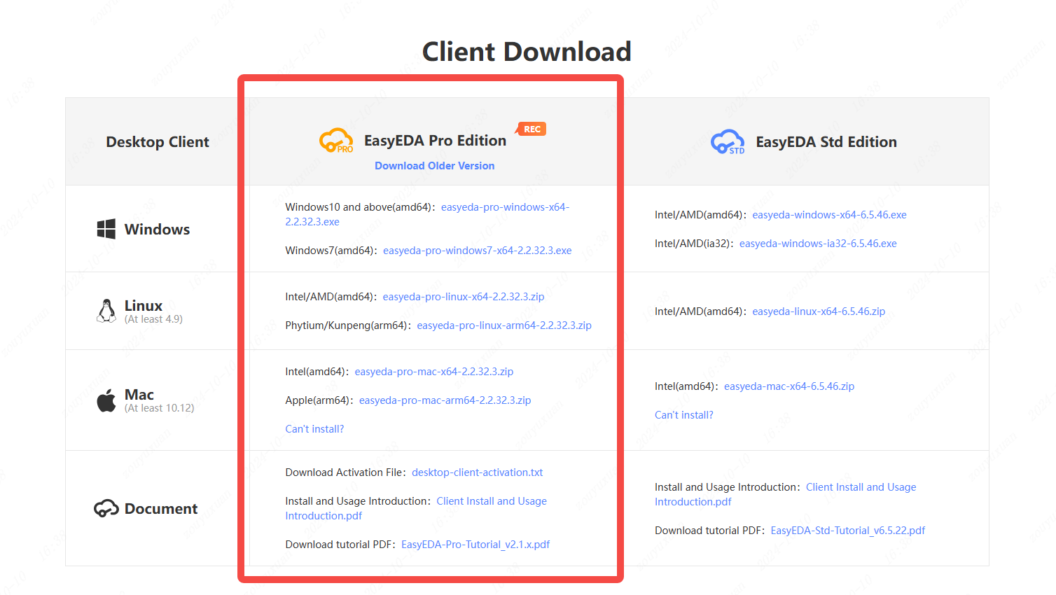
Visit the website: https://easyeda.com/page/download, and select the download link corresponding to the client version of the system (here, taking Windows 11 as an example).
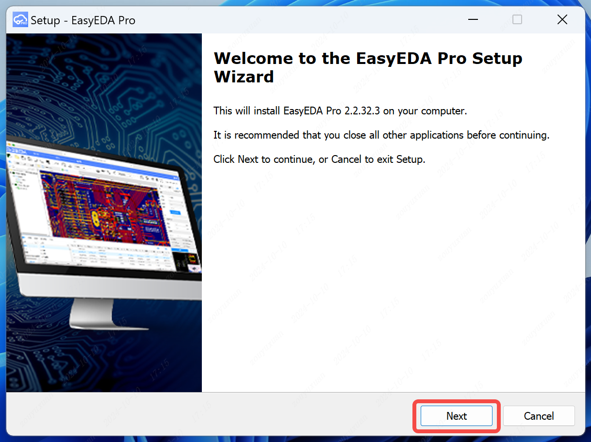
Double-click the downloaded installation package with the mouse to open it and install it by following the steps.
Activation file free download address:https://easyeda.com/page/desktop-client-activation
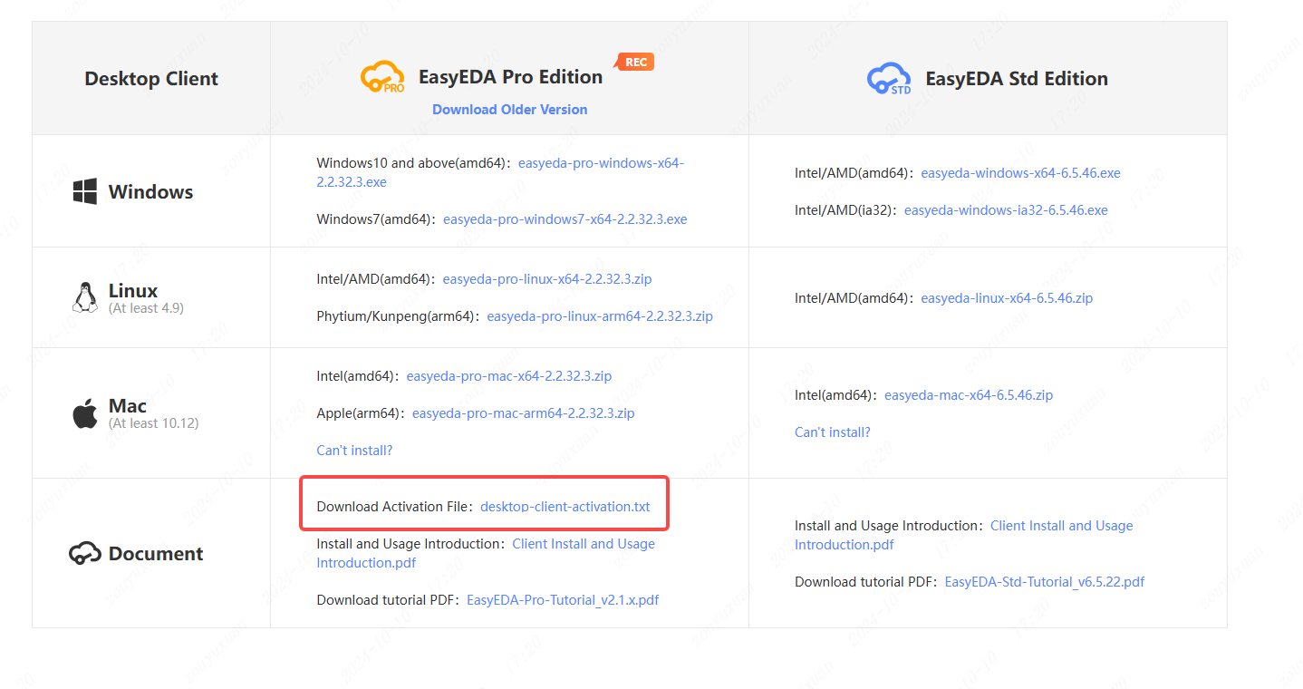
when you open the desktop client first time, it will open a activate dialog, you can download the activation file to activate.
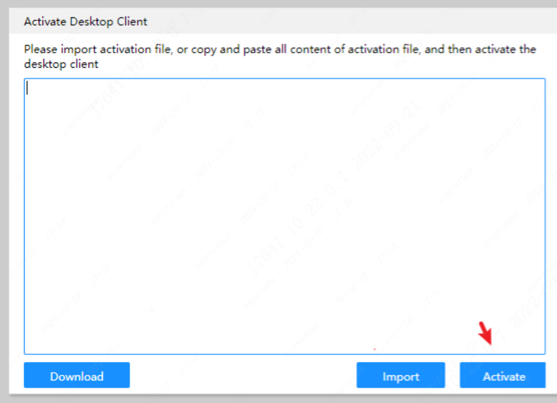
In case of relevant problems, please refer to Desktop Client FAQ
Use online
Directly access the website: https://pro.easyeda.com/editor (It is recommended to use the latest Google or Edge browser), and choose "Register" or "Login" on the upper right corner of the page.
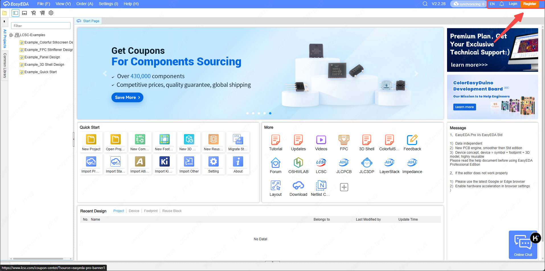
Interface introduction
The main page of the professional edition of easyeda.
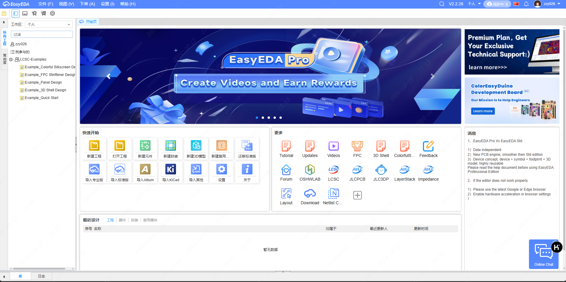
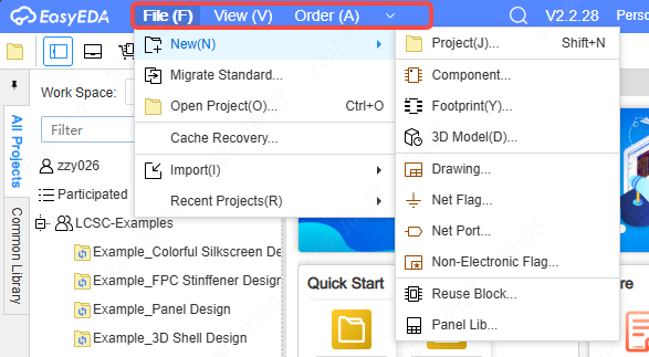
In the top menu, you are capable of undertaking relevant operations such as the creation and import/export of engineering files, the establishment of components, drawings, and panels, the switch of views, the order placement service of JLCPCB, and the configuration of EDA functions, etc.
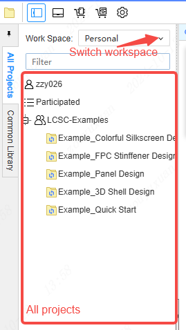
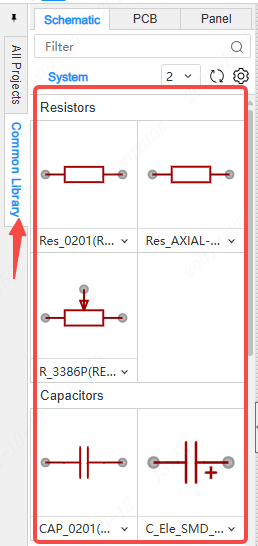
On the left panel, you can view all the projects of the current user, switch workspaces, and access the commonly used libraries for "Schematic", "PCB", and "Panel".
The editor contains a list of commonly used shortcuts and quick links to frequently used websites.

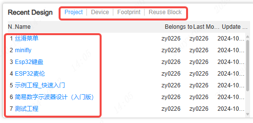
In the bottom panel, you can view the most recently designed projects, devices, packages, and reusable modules.
Draw device library
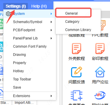
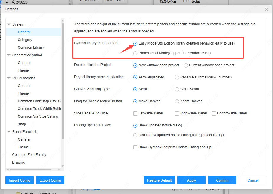
Firstly, within Settings - System - General, switch the Symbol Library Management to the Simple Mode.
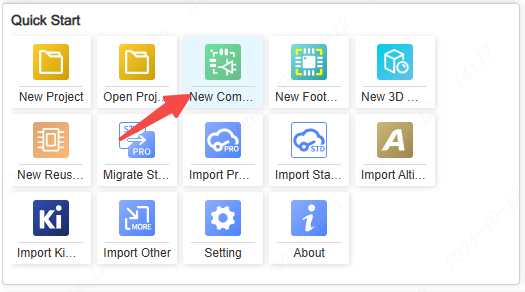
In the Quick Start window located in the middle of the editor, click the "New Component" function.
In the emerging "New Device" window, the device's attribution, name, classification, and description can be configured. (Here, taking a surface-mounted capacitor as an example)
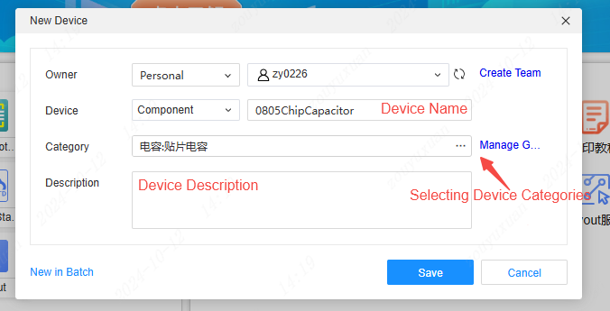
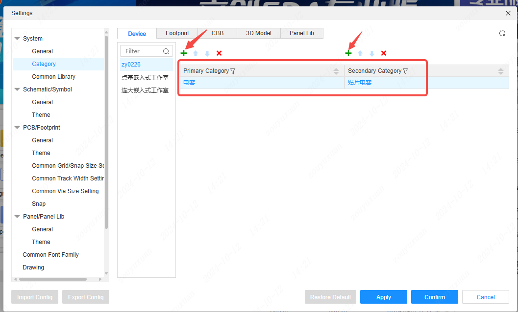
It is possible to click on "Manage Categories" and conduct the classification management of components in the emerging settings window.
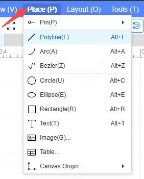
Upon clicking "Save", one will be redirected to the symbol editing interface. Click on "Place" in the top menu and select the required function for symbol drawing.
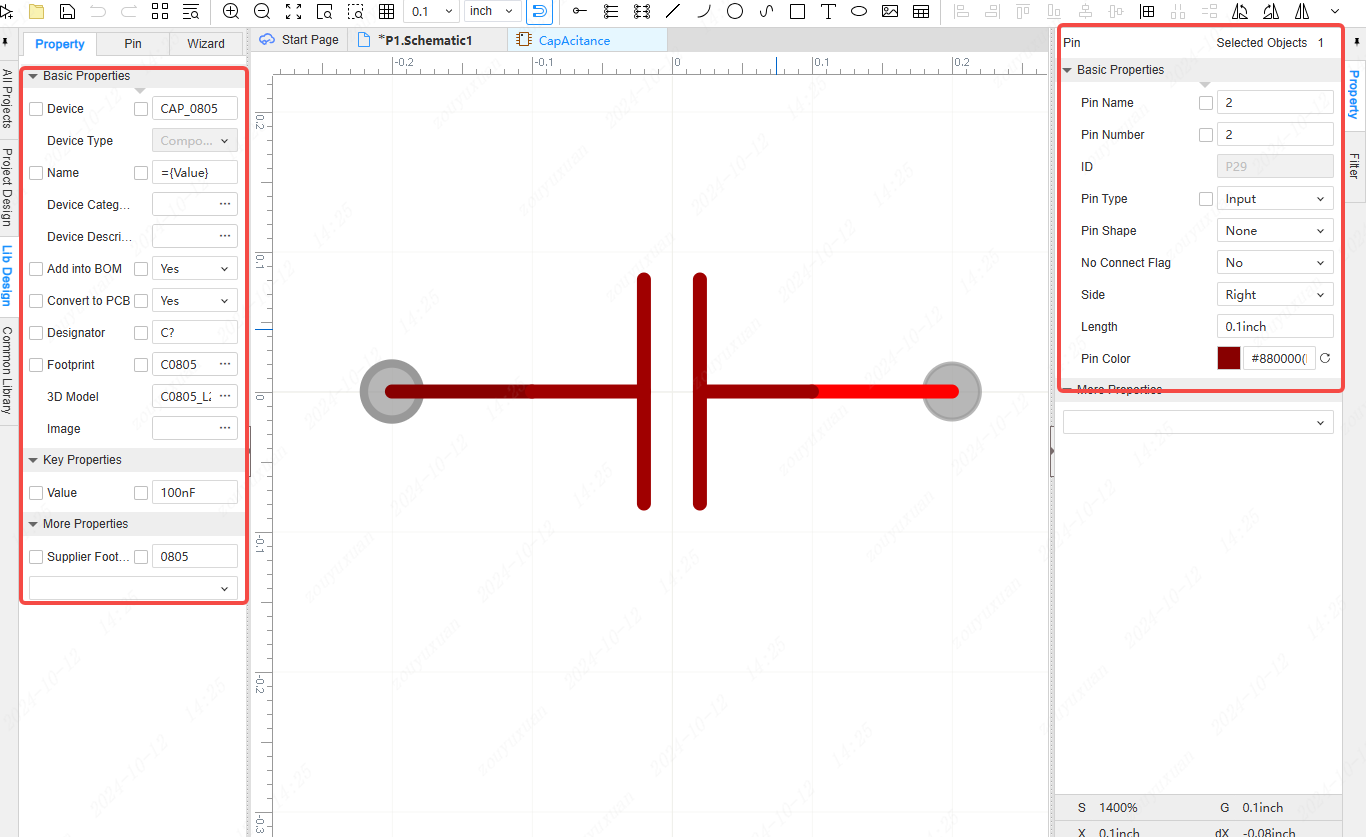
After the device symbol has been drawn, the related attributes of the device can be modified on the left panel, and the related attributes of the selected object can be modified on the right panel.
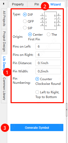
In addition to manually drawing symbols, the Professional version of LCEDA also supports generating symbols quickly using wizards.
By clicking on "File - Save All" (shortcut CTRL + S), the components drawn by oneself can be found in the component library of the bottom menu.

Draw package library
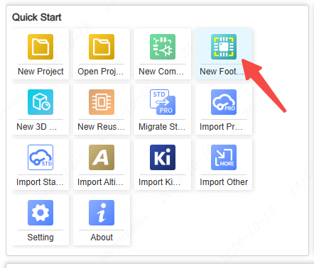
In the Quick Start window located in the middle of the editor, click on the "New Footprint" function.
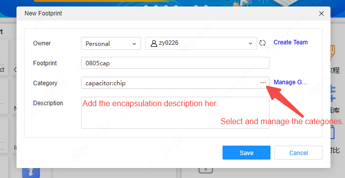
In the popped-up "New Footprint" window, it is feasible to configure the name, category and description of the package.
After clicking "Save", one will be redirected to the Package Editing page. By clicking on the "Place" option in the top menu, or choosing the quick selection function in the top toolbar, the required drawing functions can be selected.
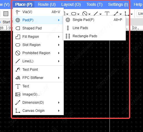
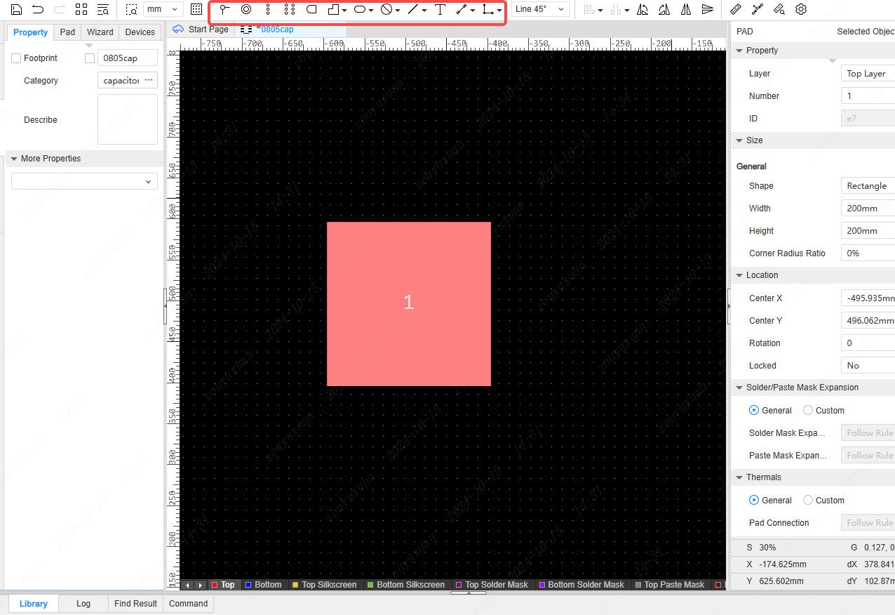
Click on "Place - Pad - Single Pad", and then left-click on the canvas with the mouse to place the pad (right-click to cancel the placement).
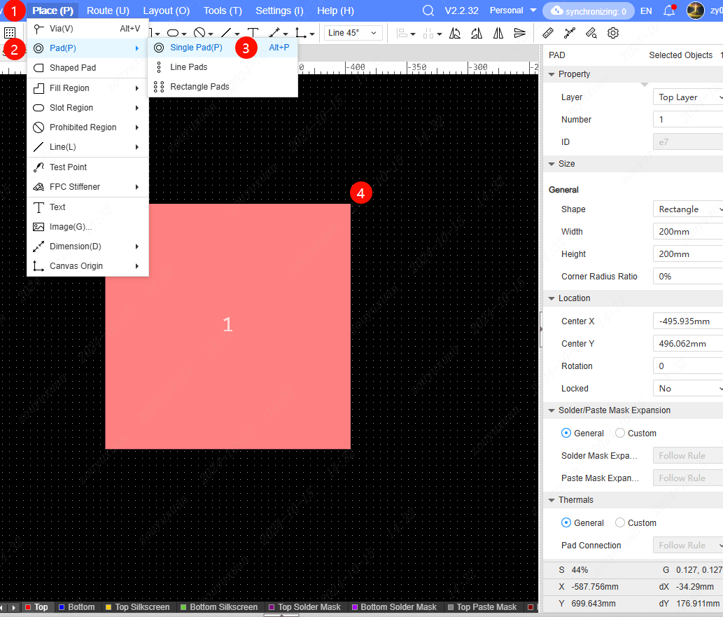
Left-clicking on the pad with the mouse can enable the modification of object properties on the right panel. When no object is selected, the right panel is for modifying the properties of the canvas document.
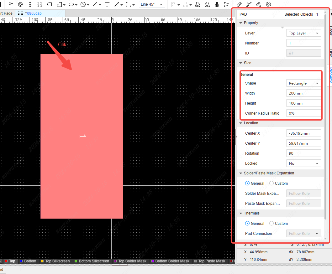
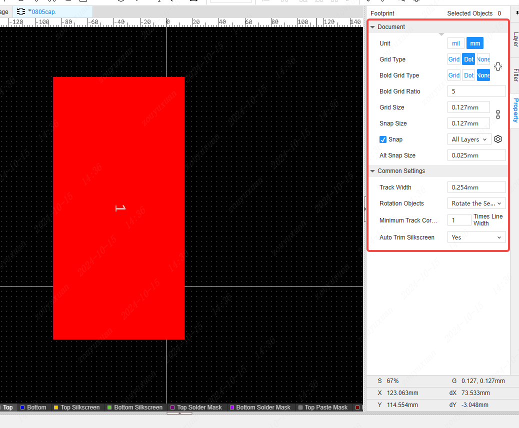
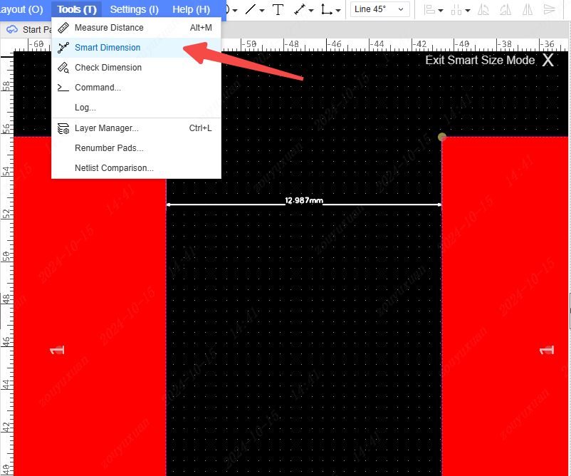
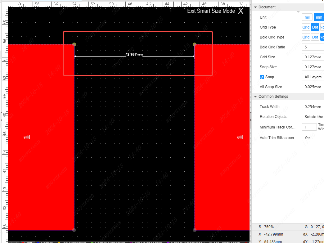
When placing the second pad, one can input the distance between the two pads, or modify the distance in the "Tools - Smart Dimension" mode.
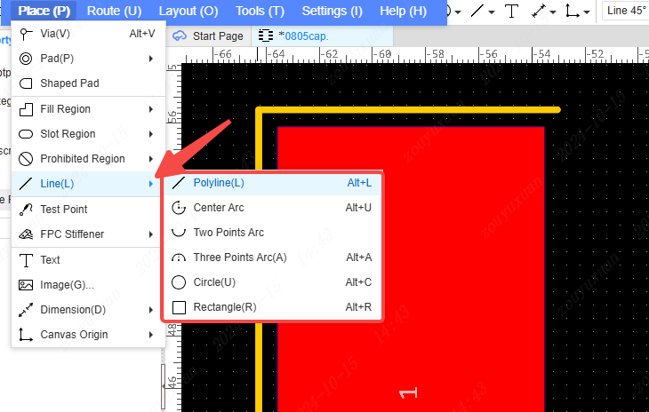
Click on the "Layer" on the right panel, select the "Top Silk Screen Layer", and then click on "Place - Line - Polyline" to draw the package silk screen.
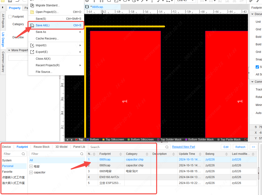
After clicking on "File - Save All" (shortcut keys CTRL + S), the device package drawn by oneself can be found in the Package Library at the bottom menu.
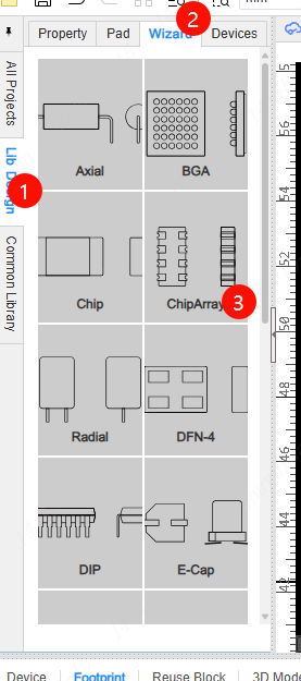
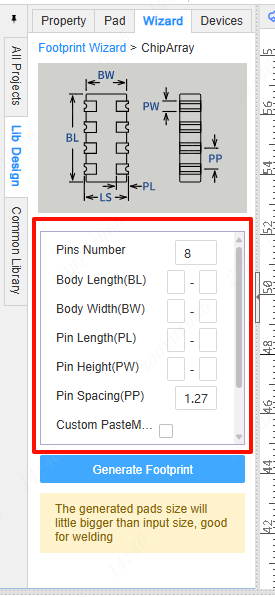
Apart from manually drawing the package, the EasyEDA Pro also supports the rapid generation of device packages by using a wizard. Click on "Library Design - Wizard" in the left panel, then select the desired package type. After filling in the package attribute values in the package window, the device package can be generated.
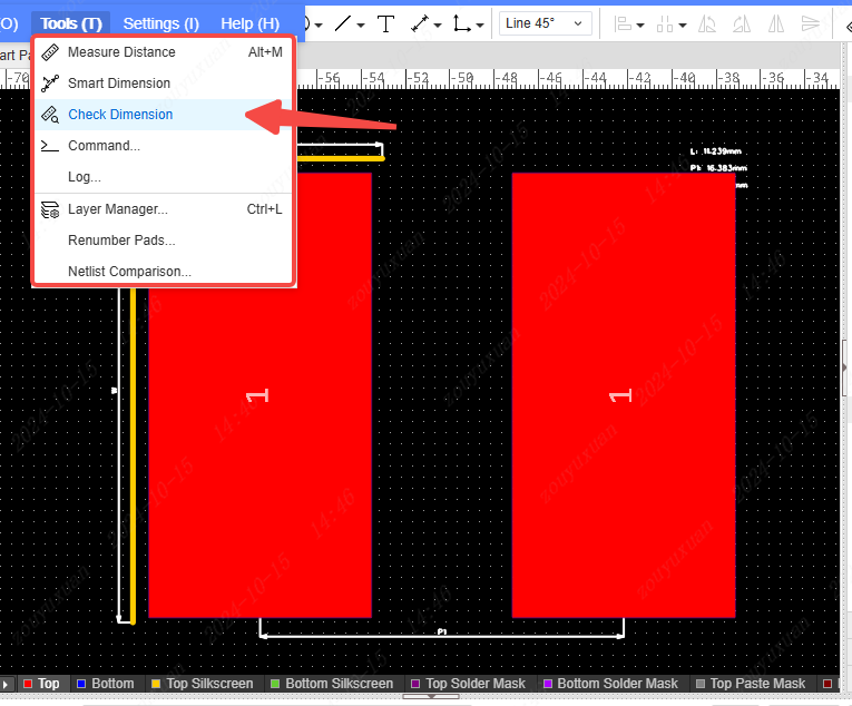
After completing the drawing of the device package, click on "Tools - Check Dimensions" to display the package dimension data.
Create a new project
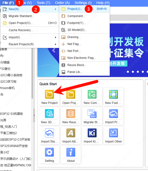
Click on "File" - "New" - "Project" or click on the "New Project" icon in the "Quick Start" window located in the middle of the editor.
In the emerging "New Project" window, the ownership, name, link and description of the project can be modified.
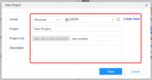
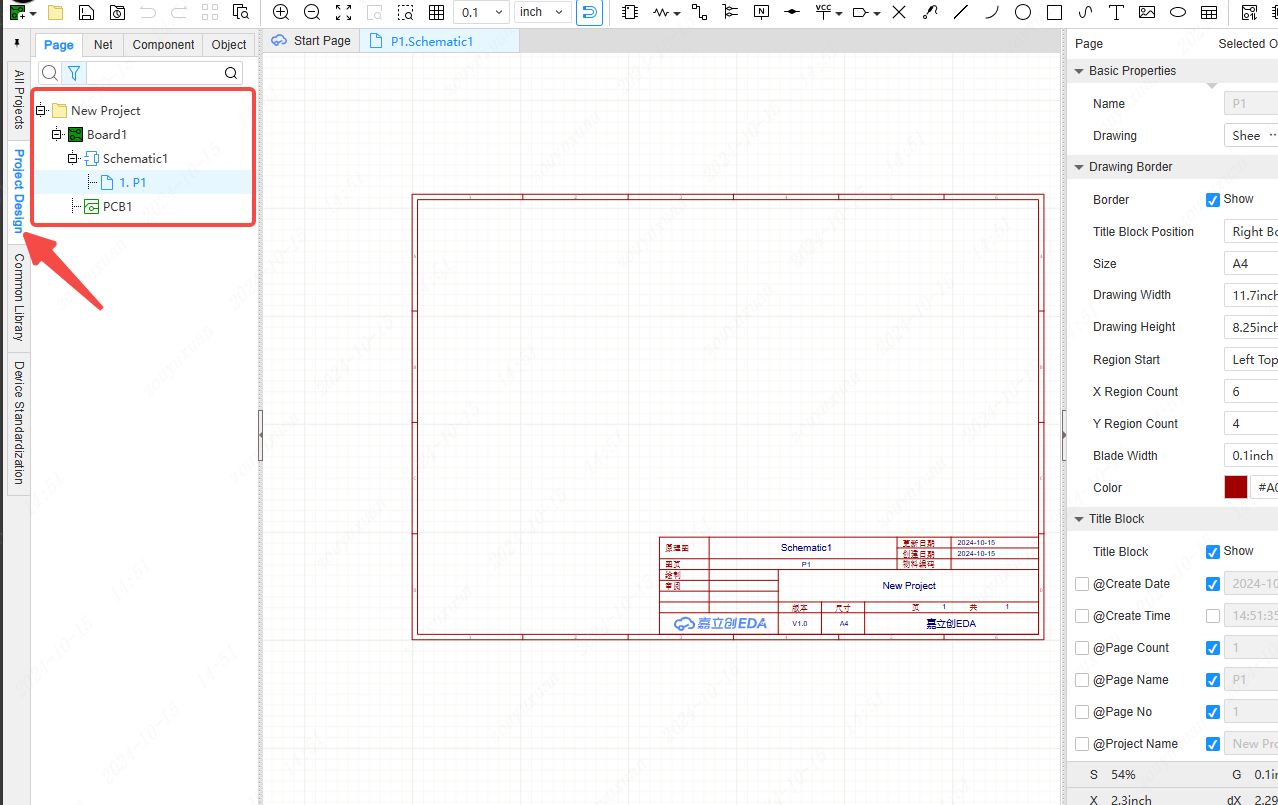
Upon clicking "Save", one will be redirected to the project design page, where the content of the current project is available in the engineering design section of the left panel.
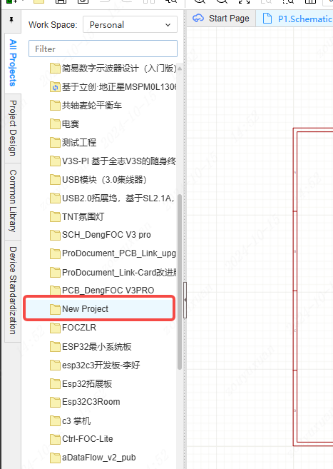
The newly created project can be observed in all the projects within the left panel.
Draw schematic
Create a new schematic
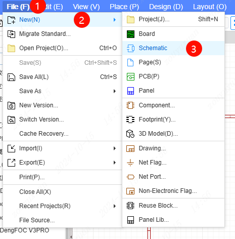
- Method 1: File - New - Schematic
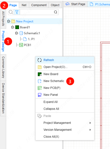
- Method 2: Right-click on the drawing page in the engineering design, and then click "New Schematic".
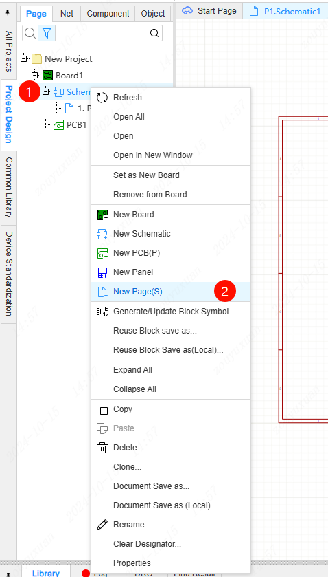
It is possible to create a new drawing page by right-clicking on the schematic within the board.
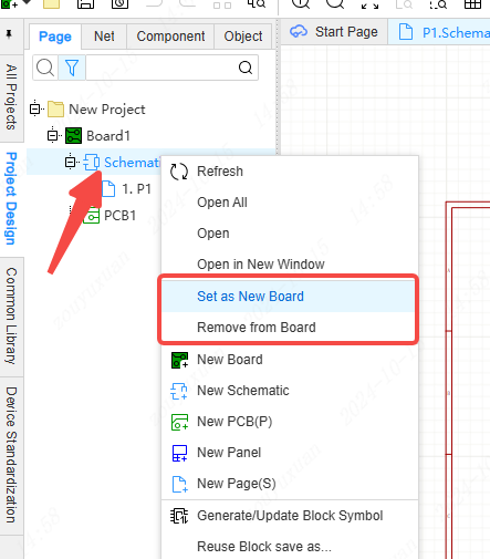
It is feasible to right-click on the schematic outside the board and select either "Set as Existing Board" or "Set as New Board".
Place device
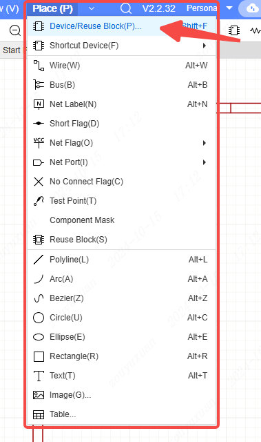
Method 1: Top Menu - Place - Devices/Reusable Block
Method 2: Top Toolbar - Components

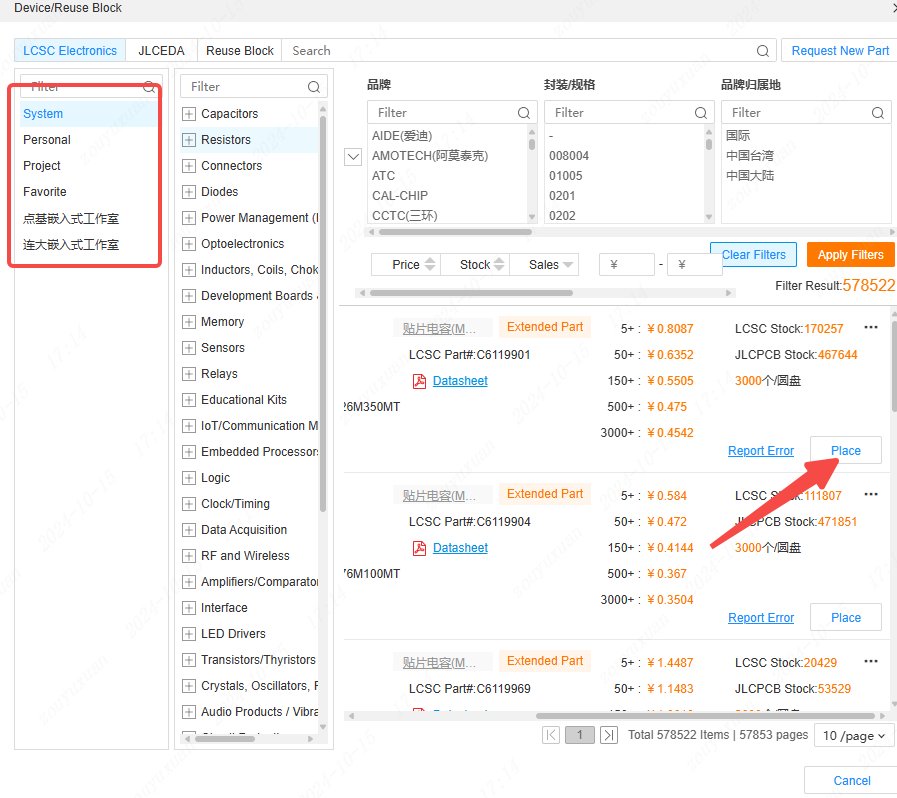
In the pop-up window of "Devices/Reuse Block", the source of the device can be selected on the left side (previously created devices can be chosen), and after finding the required device on the right side, click "Place".
Method 3: Bottom Panel - Library - Components
Select the required device in the bottom pop-up window. The symbol, package, physical image, and 3D model of the device will be displayed in the right window. After confirmation, click "Place" with the left mouse button.

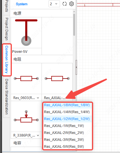
The common libraries on the left panel contain components with high usage frequencies for selection. By clicking the dropdown pop-up window below the component, the component type can be changed.
Device layout
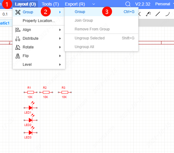
Left-click and select the devices that need adjustment with the mouse, then click on "Layout" in the top menu bar and choose the required layout function.
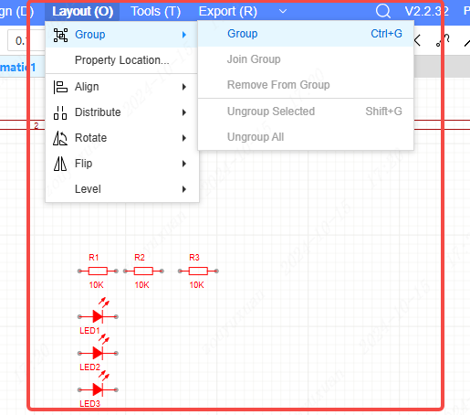
The combination function can group the devices you select as a whole. After being combined as a whole, when performing operations such as dragging and rotating, the relative positions of each device within the group can be ensured to remain unchanged.
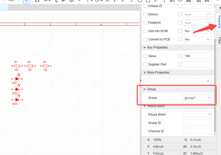
After the combination is completed, the combination properties can be viewed in the property column on the right side panel.
Other functions in the device layout are all good assistants for you to optimize the placement of devices.
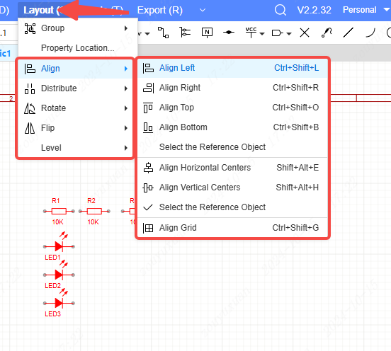
For more information on device layout, please refer to: Schematic Design - Layout - Align
Draw wires
Wires are employed when designing a schematic to connect the networks with electrical attributes among various devices.
Click on "Place - Wire" in the top menu bar.
Shortcut keys: Alt + W (for Professional Edition theme configuration) or W (for Standard Edition theme configuration)
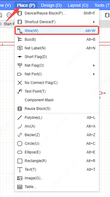
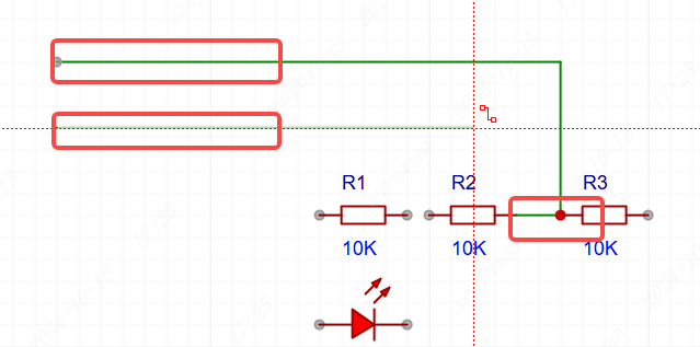
During the drawing process, left-clicking of the mouse determines the line segment, and right-clicking cancels the operation. The unfinished portion is a semi-transparent line segment.
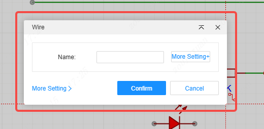
When entering the wire drawing state, the name of the wire can be set by pressing the TAB key.
Modify components
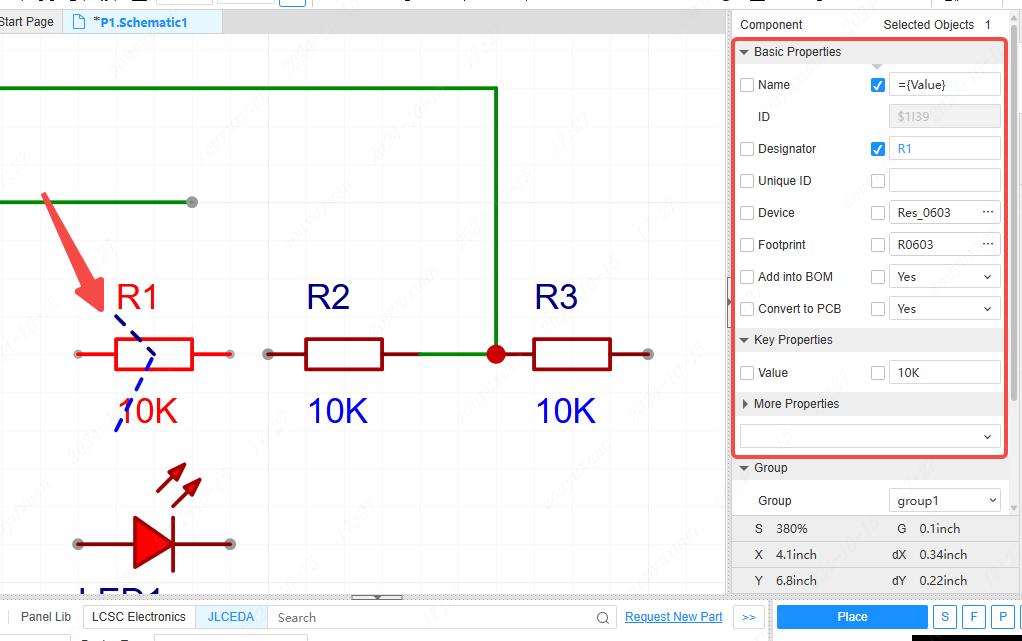
For the components that have been placed, you can select them by clicking with the left mouse button and then make amendments in the property column on the right side.
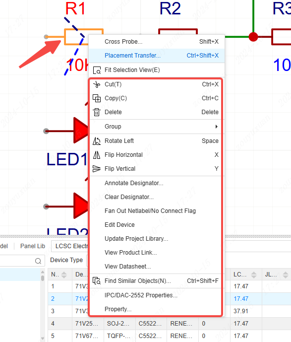
Likewise, you can right-click on the component you wish to modify and carry out the modifications in the pop-up window.
Convert schematic to PCB
Upon the completion of the schematic drawing, clicking on "Design - Check DRC" enables a holistic inspection of the schematic.
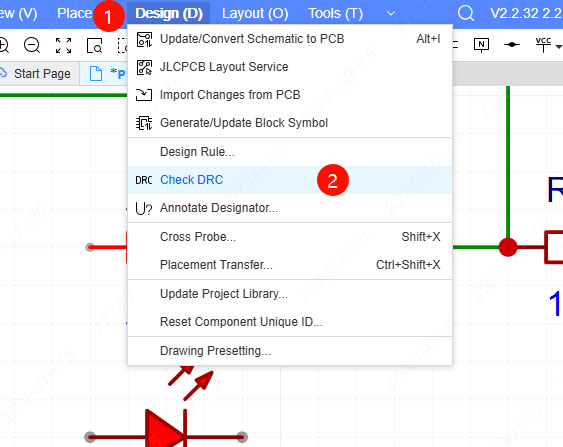
The inspection results will be presented in the DRC column at the bottom panel. After modifying based on the inspection results, clicking the "Check DRC" button on the left allows for viewing the new inspection outcomes.

In case "Standardization of Devices Recommended" emerges, click on "Device Standardization" on the left panel for modification.
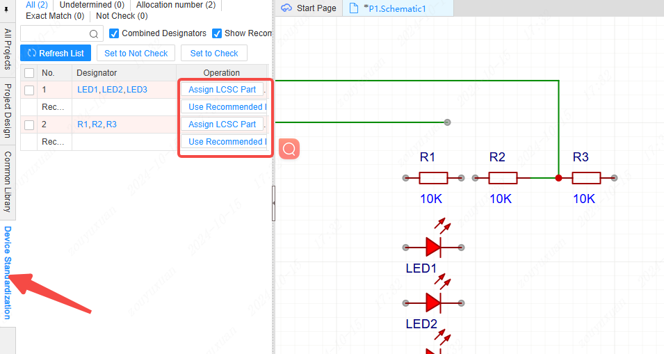
For areas of uncertainty, refer to the video tutorial: Schematic - Left Panel - Device Standardization
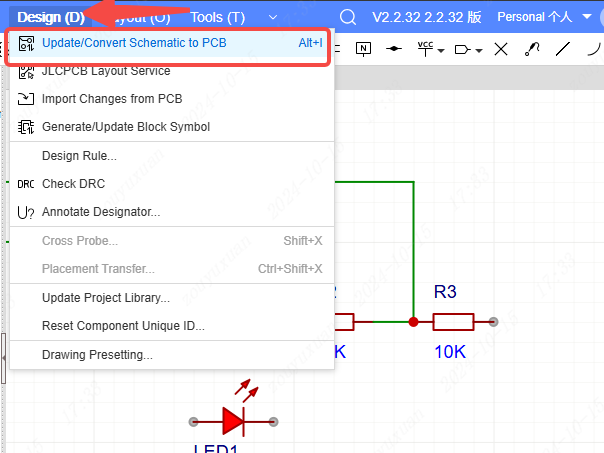
Once the overall inspection of the schematic is completed, clicking on "Design - Update/Convert Schematic to PCB" in the top menu bar enables the importation of new content or modifications in the schematic to the PCB.
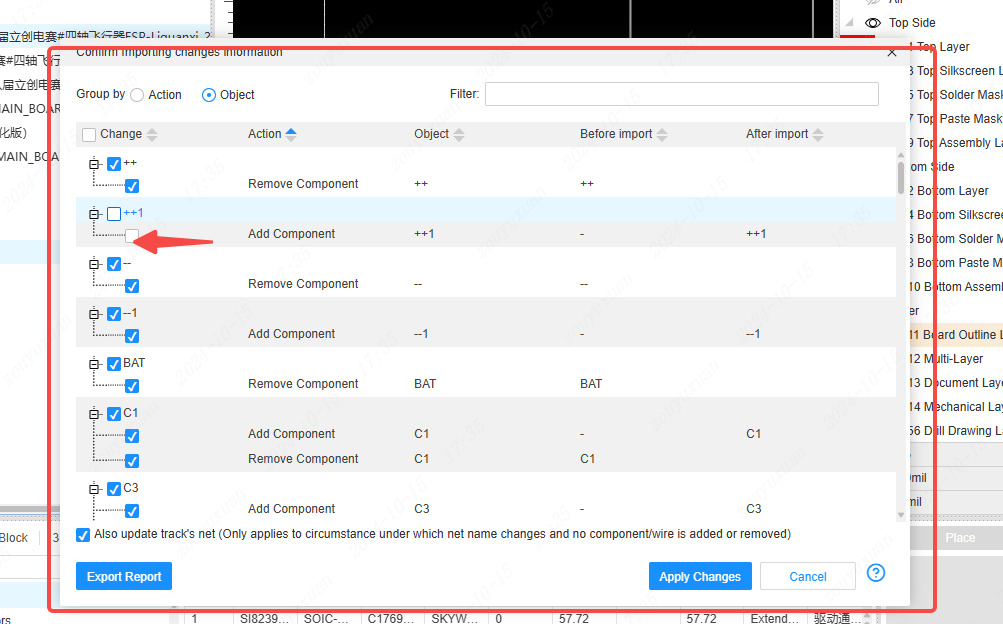
If there are no issues with the schematic and it has been successfully imported to the PCB, a pop-up window labeled "Confirm Import Information" will appear. By default, all changes are checked. If certain changes are not required, they can be unchecked on the left. After confirming the changes, clicking "Apply Changes" accomplishes the conversion from schematic to PCB.
Draw PCB
Create a new PCB
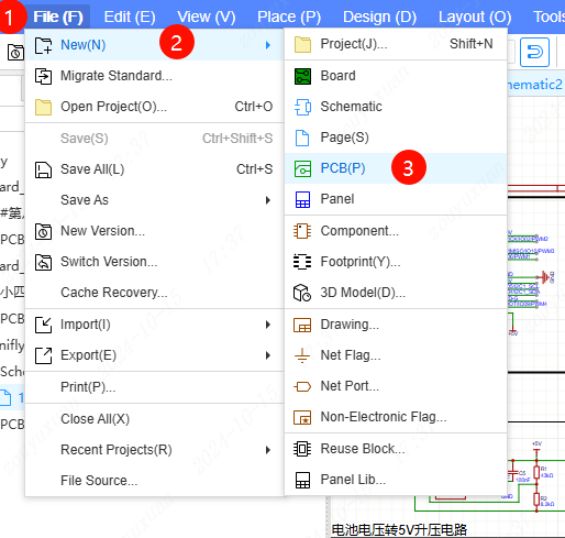
Method 1: File - New - PCB
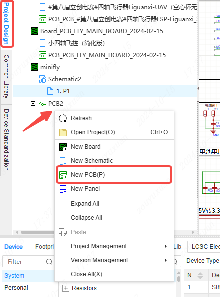
Method 2: Right-click on the page of the engineering design and click "New PCB".
It is possible to right-click on the PCB outside the board and select "Set as Existing Board" or "Set as New Board".

Draw board frame
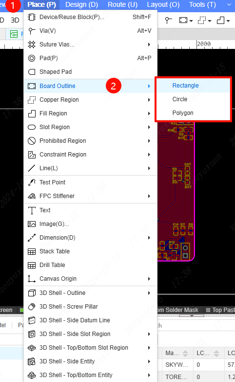
Click on the top menu bar, select "Place" followed by "Board Outline", and choose the required shape for the board outline to be drawn.
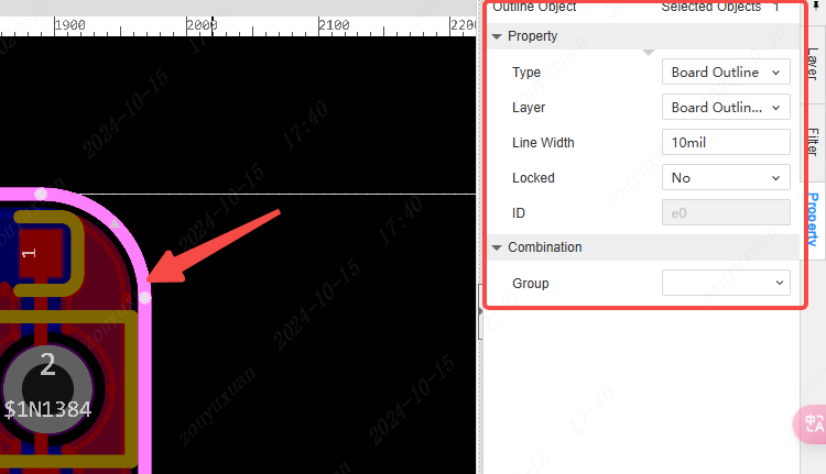
For the already drawn board outlines, the board outline can be selected by left-clicking with the mouse, and adjustments can be made to it in the property column on the right panel.
Set design rules
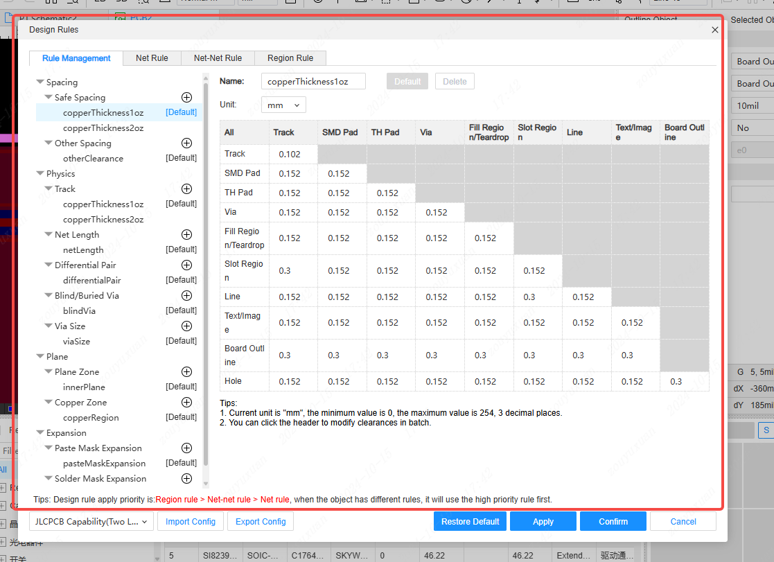
Design rules are employed to establish the fundamental design principles for PCB. Inputting a safe design rule within the design rules can guarantee that no design problems will arise in the PCB design.
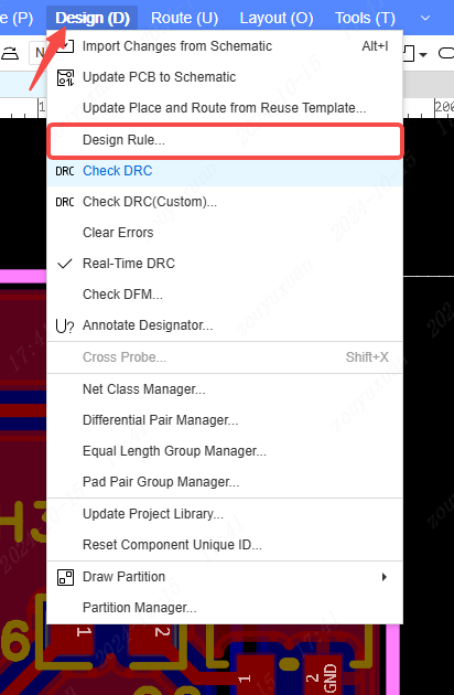
Click on the top menu bar, Design - Design Rule, and you can revise the design principles within the "Design Rules" pop-up window.
Set PCB layers
For a single or multiple components, you can frame-select them with the left mouse button, and then perform layer modifications in the property column on the right panel.
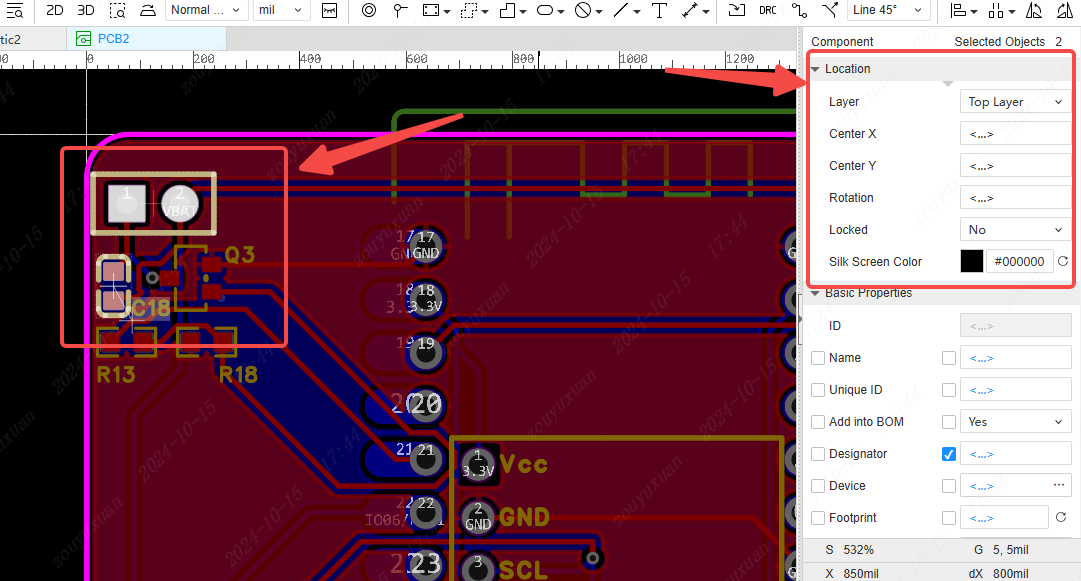
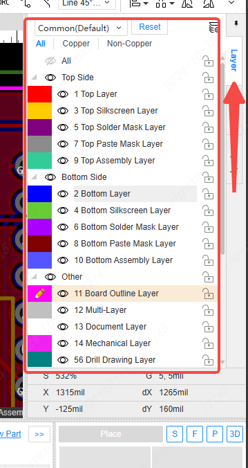
If you wish to operate on the layers, click on the layer column on the right panel. Here, you can switch and edit different layers.
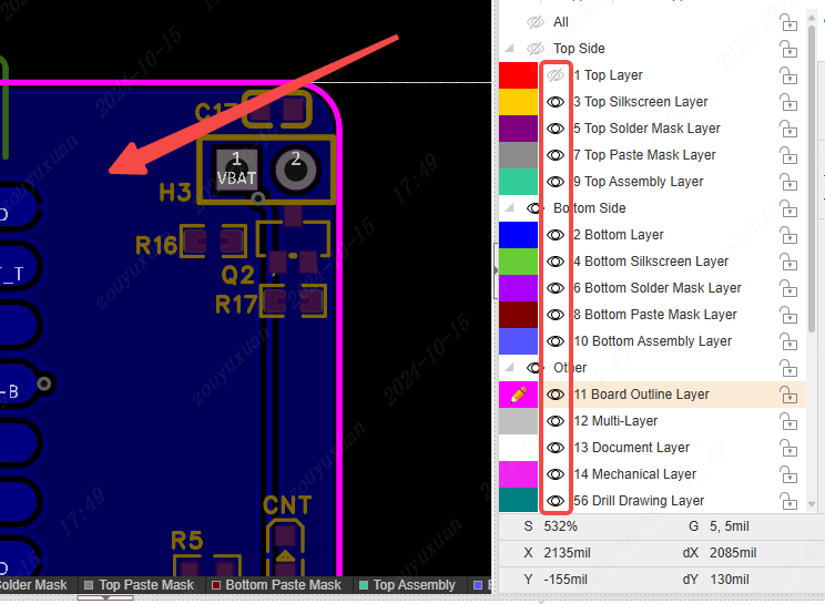
Clicking on the eye icon corresponding to the layer enables or disables the display of that layer.
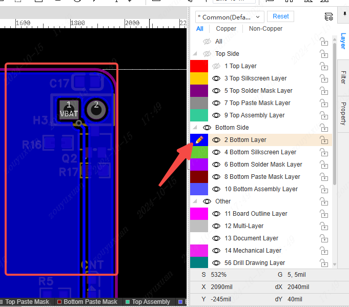
Clicking on the color identification area of the layer switches the pencil icon to the corresponding layer, indicating that the layer is active and has entered the editing state. Operations such as wiring can be performed. Layer switching can also be carried out in the bottom column of the page.
Clicking on the lock icon of the layer will lock the layer, and elements belonging to that layer will not be movable by the mouse.
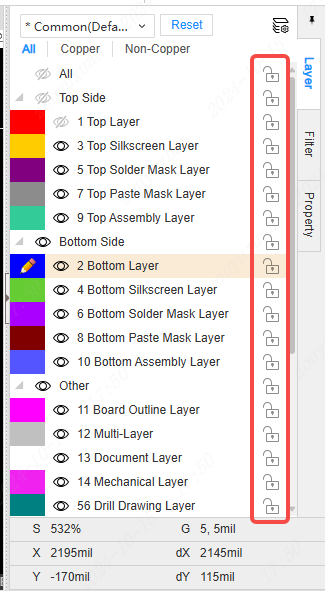
For more information regarding PCB layers, please refer to: PCB Design - Tools - Layer Manager
Import schematic changes
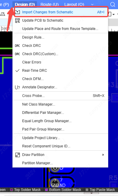
If the schematic diagram undergoes changes, one can click on the top menu bar "Design - Import Changes from Schematic" to synchronize the changes.
Component layout
Use the left mouse button to box-select the components that need adjustment. Click "Layout" in the top menu bar and then select the required layout function.
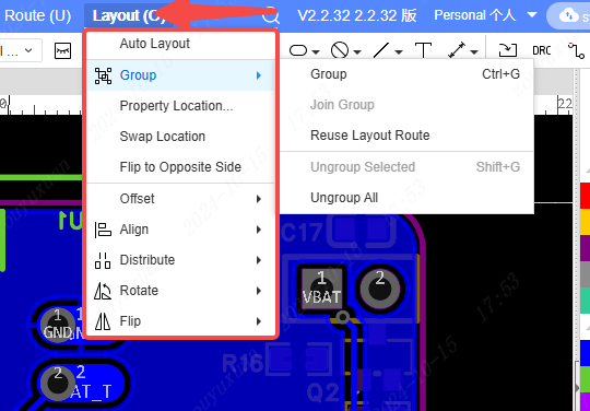
The combination function can group the components you box-select into a single entity. After being grouped into a single entity, when performing operations such as dragging and rotating, the relative positions of the components within the group can be ensured to remain unchanged.
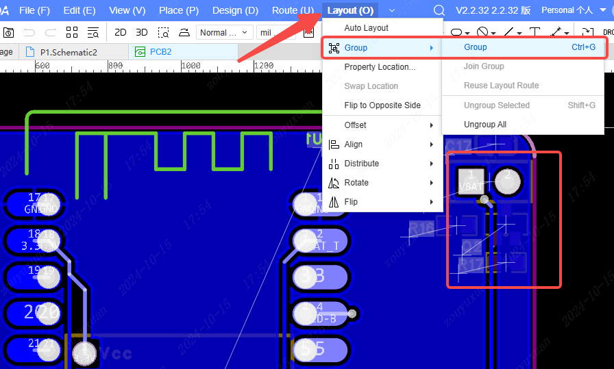
After the combination is completed, the combined properties can be viewed in the property column on the right side panel.
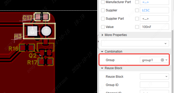
Other functions in the component layout are all good assistants for you to perfect the placement of components.
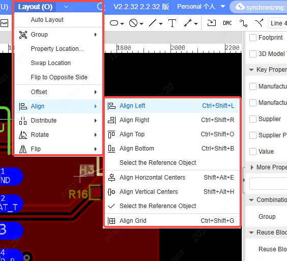
For more information on component layout, please refer to: PCB Design - Layout - Align
Component routing
Click on the top menu bar and choose "Wiring - Single-path Wiring" to enter the single-path wiring working mode.
The shortcut key is ALT+W (for the EasyEDA Pro theme configuration)
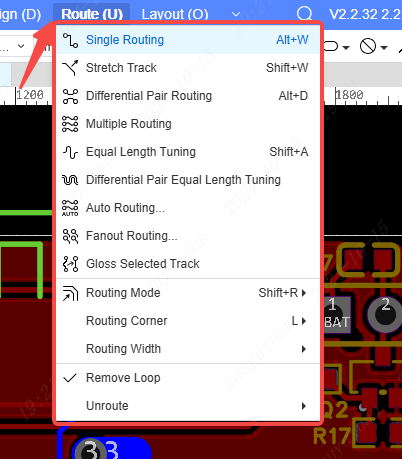
When conducting wiring, it will be performed on the currently edited layer. During the wiring process, left-clicking the mouse adds an inflection point, and right-clicking the mouse cancels the wiring.
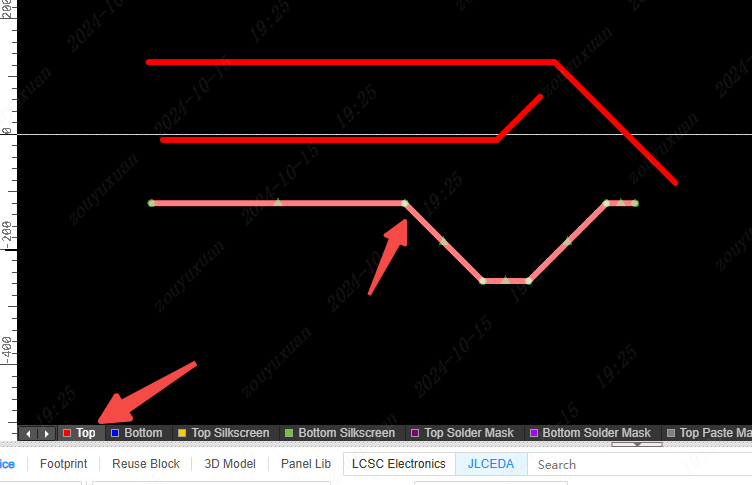
For more information regarding component wiring, please refer to: PCB Design - Wiring - Single-path Wiring
Add copper
If you wish to retain the entire copper foil area for grounding or power connection purposes, you can employ the "Copper Pour" function.
Click on the top menu bar and choose "Place - Copper Pour Area" or click the copper pour icon in the top toolbar.
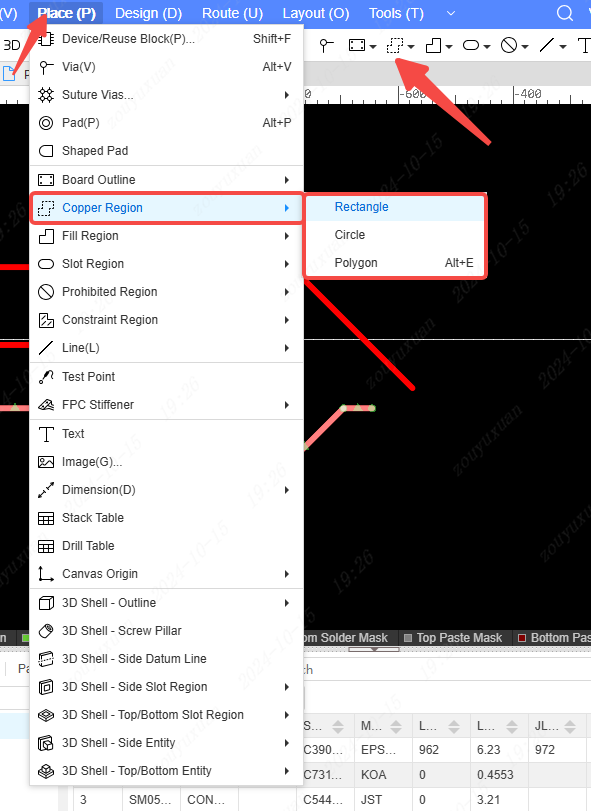
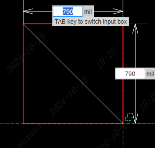
Click the left mouse button to commence drawing the copper pour area, and click the left mouse button again to confirm the copper pour area. Click the right mouse button to cancel the copper pour operation.
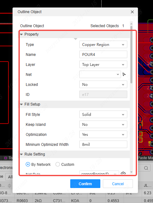
After the drawing is completed, the network that the copper pour area contacts is automatically set. You can modify the layer, network, and other attributes of the copper pour area through the pop-up window that appears.
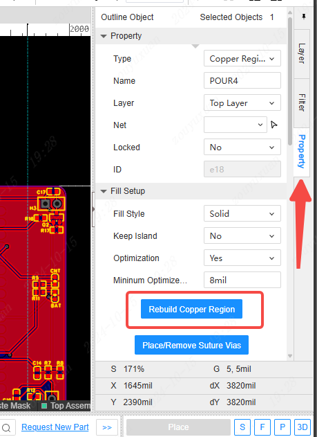
If the copper pour area has been modified, click on the copper pour area with the left mouse button, and the "Rebuild Copper Pour Area" option will be available in the property column on the right side of the panel.
For more information regarding the addition of copper pours, please refer to: PCB Design - Place - Copper Pour Area
DRC check
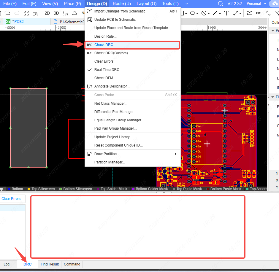
After the PCB has been drawn, a comprehensive inspection is required. Click on the top menu bar "Design - Check DRC", and the inspection results will be presented in the DRC window at the bottom of the menu bar.
Modify silk screen
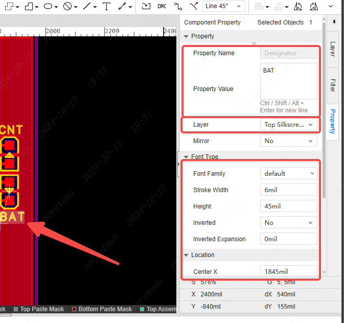
If it is desired to modify the content of the silk screen, select the silk screen object with the left mouse button and make the relevant modifications in the property column of the right panel.
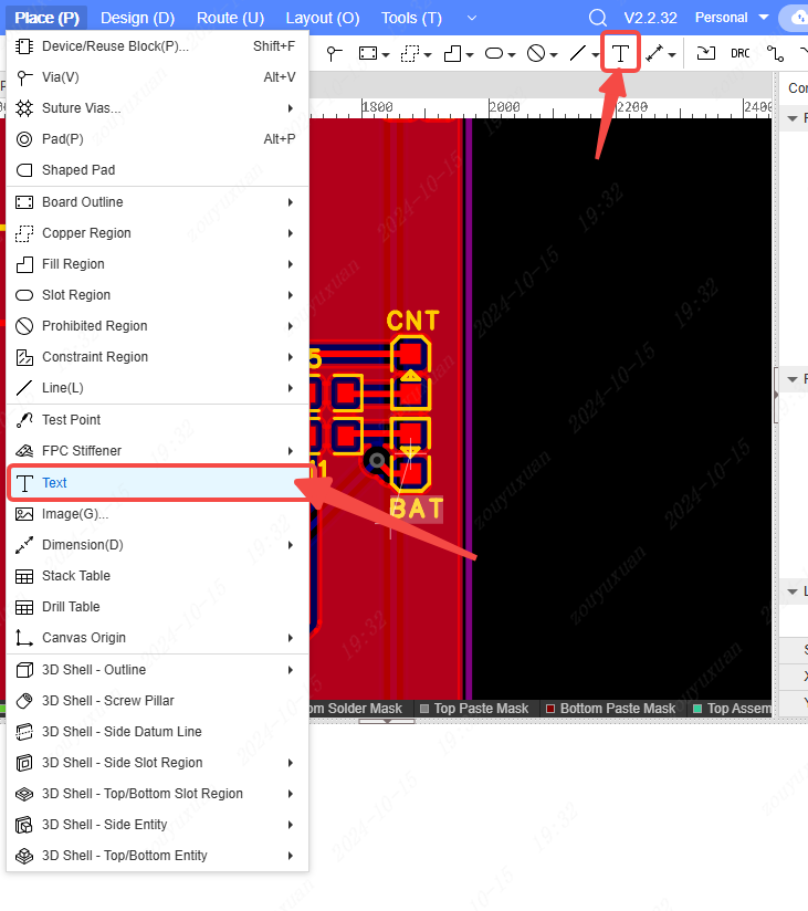
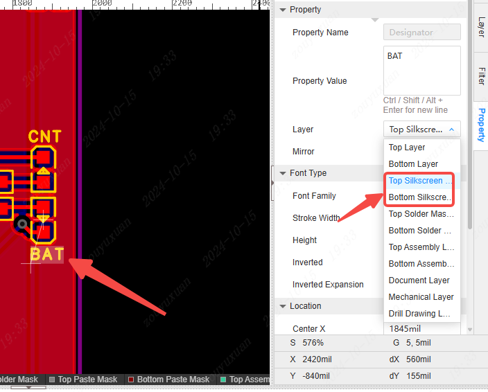
If it is intended to add a new silk screen, the font can be placed and then the layer can be changed to the silk screen layer.
Output manufacturing files
Export BOM
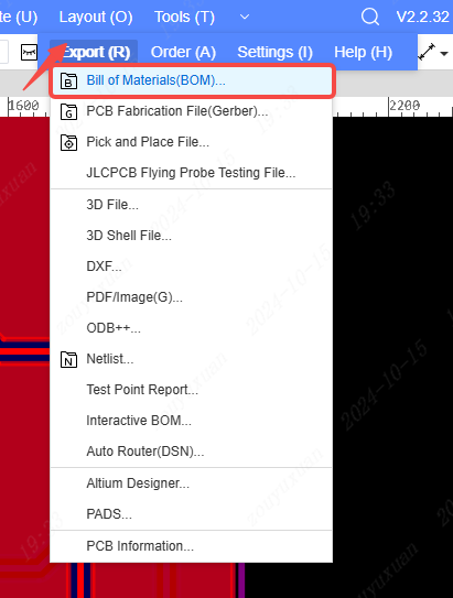
Click on the top menu bar and choose "Export - Bill of Materials (BOM)".
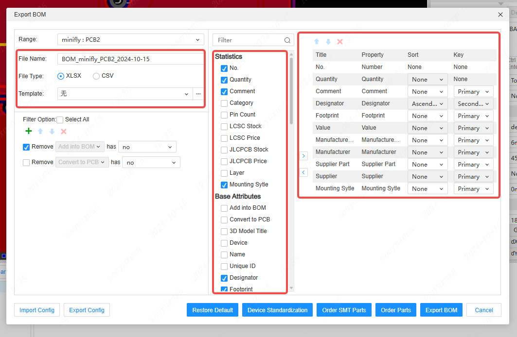
In the pop-up window "Export BOM", it is possible to modify the file type, name, and the attribute values of the BOM to be exported.
Export PDF
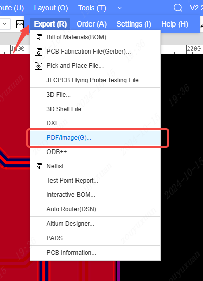
Click on the top menu bar and choose "Export - PDF/Image".
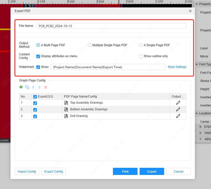
In the pop-up window "Export PDF", the PDF name, watermark, and page configuration can be modified.
Export coordinate file
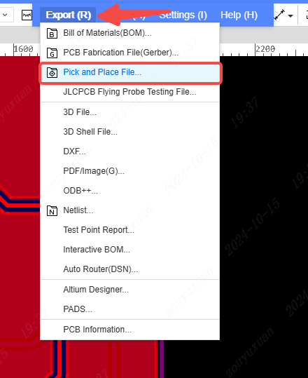
Click on the top menu bar and choose "Export - Pick and Placce File".
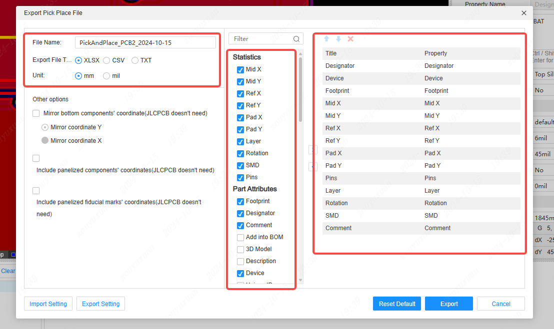
In the pop-up window "Export Pick Place File", the file type and content for export can be modified.
Export Gerber
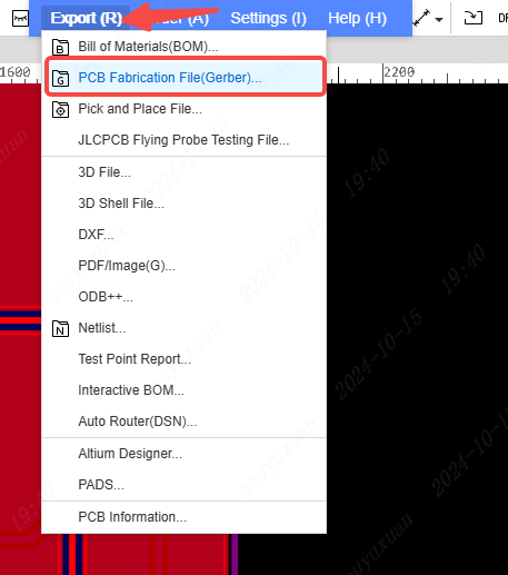
Click on the top menu bar and choose "Export - PCB Fabrication Files (Gerber)".
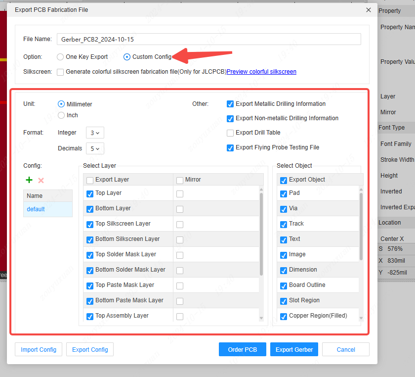
In the pop-up window "Export PCB Fabrication Files", one can click on the Custom Configuration to modify the content to be exported.
Export Step
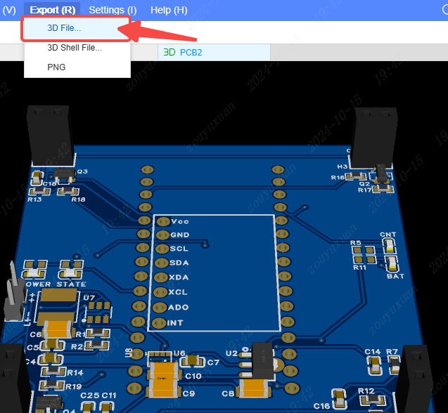
Click on the "3D" icon in the top toolbar to access the 3D preview page.

Then click on the top menu bar and choose "Export - 3D File".
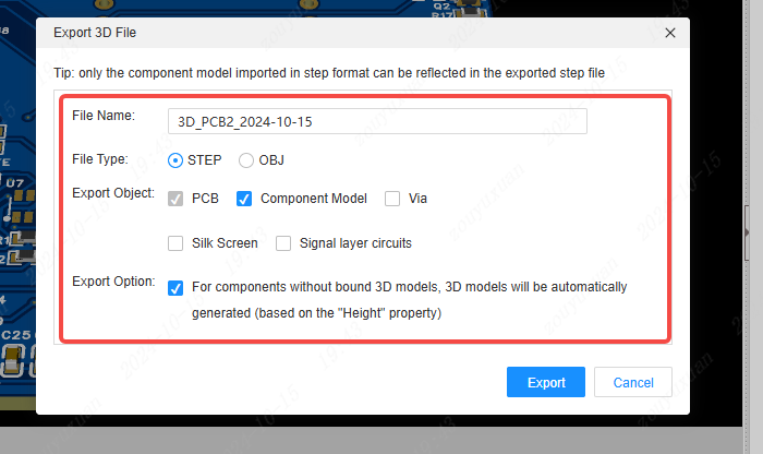
In the pop-up window "Export 3D File", the content to be exported can be modified.
Export DXF
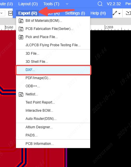
Click on the top menu bar and choose "Export - DXF".
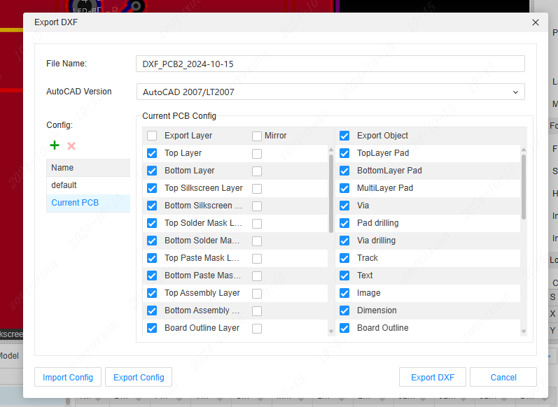
In the pop-up window "Export DXF", the file version corresponding to AutoCAD and the required configuration content can be modified.
Place an order
One-click order
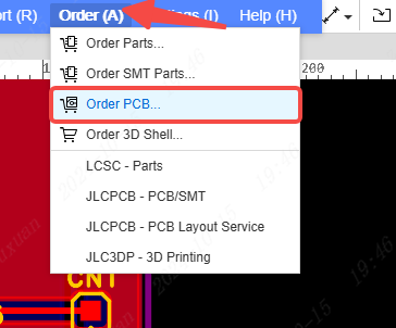
Click on the top menu bar and choose "Order - PCB Order".
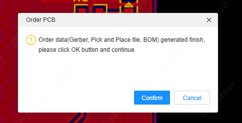
Directly click "Confirm" to enter the order page.
Upload order
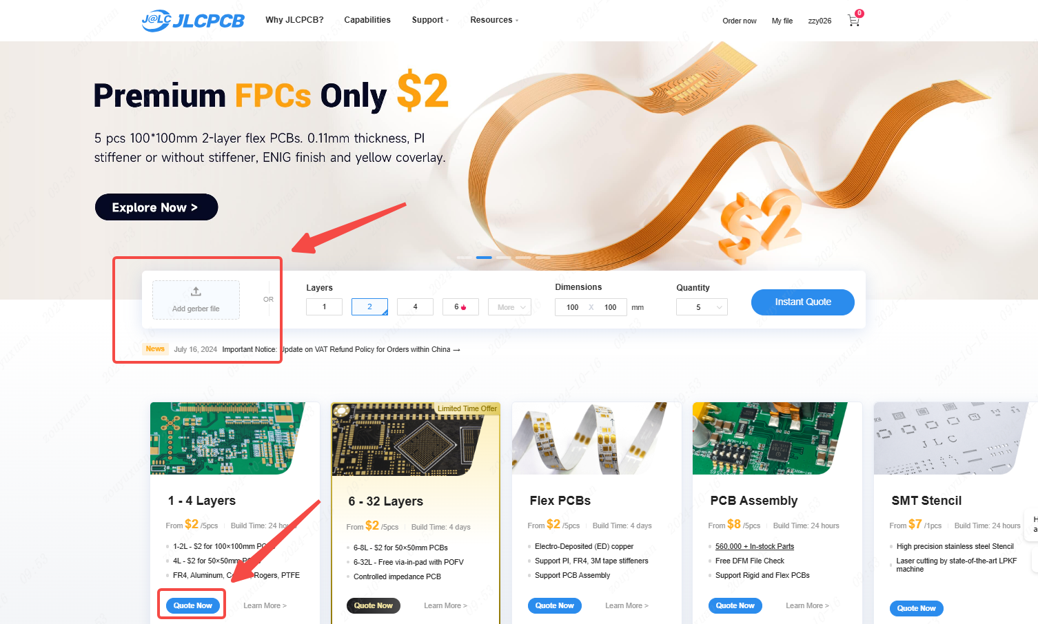
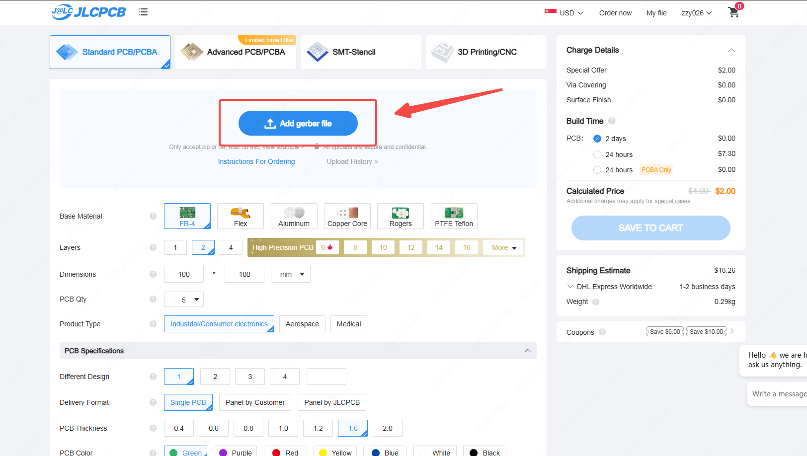
Access the website https://jlcpcb.com. Click the "Add gerber file" or "Quote NoW" button under "JLCPCB".
