Blind and Buried Vias
EasyEDA Pro already supports Place of blind and buried vias. Before the operation, let me introduce what blind and buried vias are.
Blind Vias: In the design of multi-layer board, one side of the hole is on the surface of the board, and then leads to the inside of the board. Blind vias are vias that connect the surface layer and the inner layer without penetrating the entire page. Blind vias refer to vias that connect between inner layers and are not visible on the surface of the finished board.
Buried vias: Buried vias refer to vias made in the inner layer, which are invisible to the surface and bottom layer, and are used for inner layer signal interconnection. Generally used in mobile phones and PDA boards. Buried vias can reduce the probability of signal interference, maintain the continuity of the characteristic impedance of the transmission line, and save the wiring space, which is suitable for high-density and high-speed circuit board design.
Before placing blind and buried vias, you need to add blind and buried vias in the rule settings. The premise of setting blind and buried vias is that they must be added on two-layer boards or more.
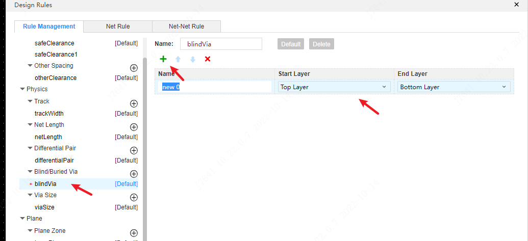
Click "+" to add blind buried via,
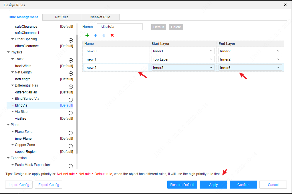
After adding, name the blind and buried vias, and select the start and end layers.
Note: When the start layer is the top layer, the end layer cannot be the bottom layer. After adding buried vias and buried vias Click OK to complete the setting of the rules for blind and buried vias.
Before placing the blind-buried via, you need to place a passer, find the properties of the via on the right panel, and select the blind-buried via just added.
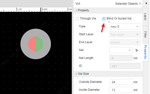
Blind vias: Top layer to inner layer 1
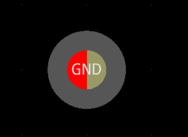
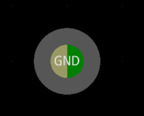
Buried vias: Inner layer 1 to inner layer 2.
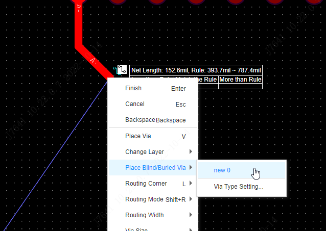
Place blind and buried vias in routing mode
Right-click to add blind-buried vias in wiring mode. When placing blind-buried vias, you need to switch to the corresponding layer to place them.
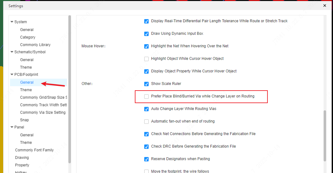
Blind and buried vias can also be placed preferentially when routing layers in the system settings.
