Cross Probe
The schematic diagram and PCB under the same board can use this cross selection for mutual positioning elements, pins, track networks, and reuse modules.
Steps:
Top Menu - Design - Cross Probe
Select components, pins, track networks, right -click menu after reuse modules -cross Probe
Select components, pins, track networks, shortcut keys after reuse modulesShift+X
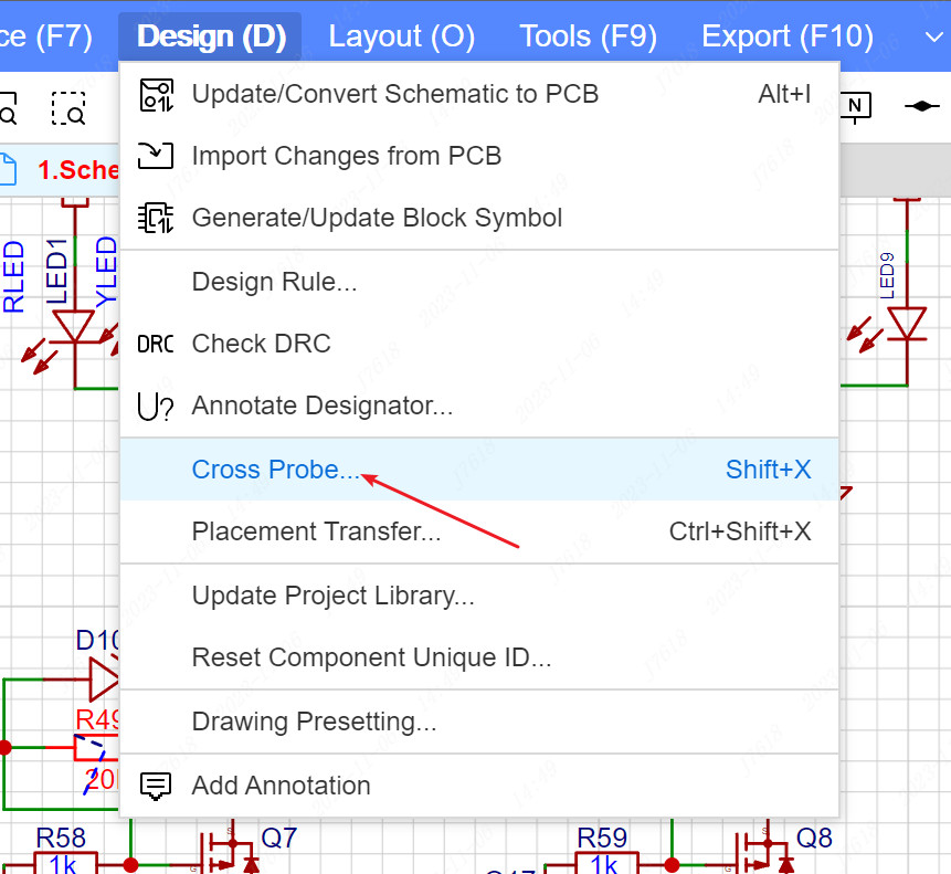
Instructions:
After selecting the component, select the cross probe function, according to the unique ID of the component, and select the PCB component that corresponds to the same ID.
After selecting the pin, select the cross -selection probe, which will highlight and select the same number in the PCB corresponding element.
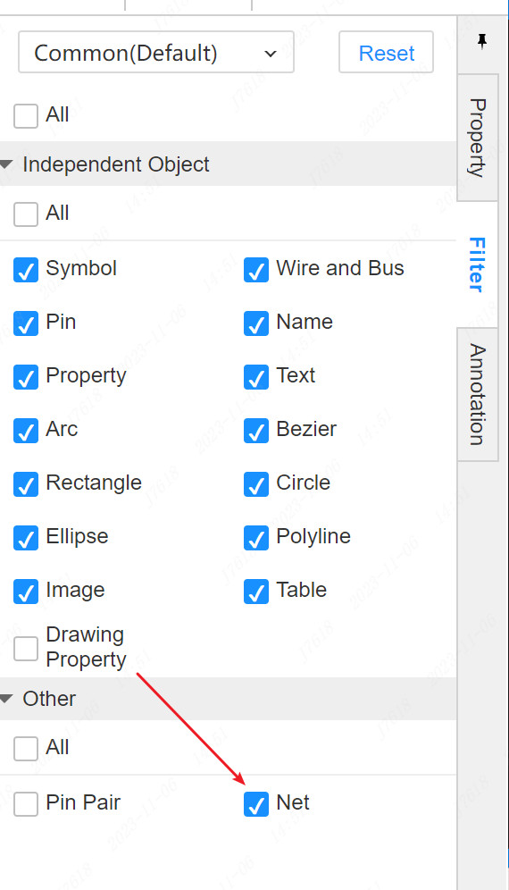
After the filter panel hooks the net, after selecting the track, net flag, net port, and net label, select the cross selection function, which will highlight and select all objects of the PCB corresponding net
- After selecting the symbol of the reuse module, select the cross selection function, which will highlight and select all components of the corresponding module in the PCB