Cross Probe
Elected a component,component pad, and net, you can use cross probe function to perform the component location of the positioning schematic diagram
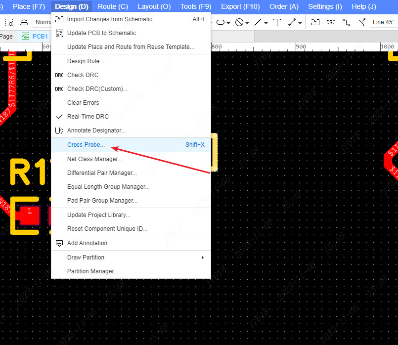
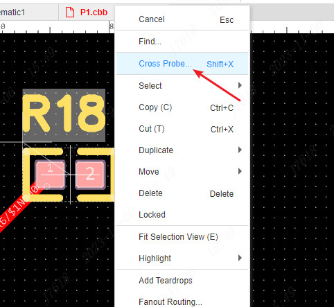
The shortcut key shift+x, or the component right -click menu for cross probe
After the PCB is selected by the object, the page of the object where the object is required in the schematic diagram will be shifted on the left map tree, the top label, and the bottom label of the reused module and the red display is displayed.Page.
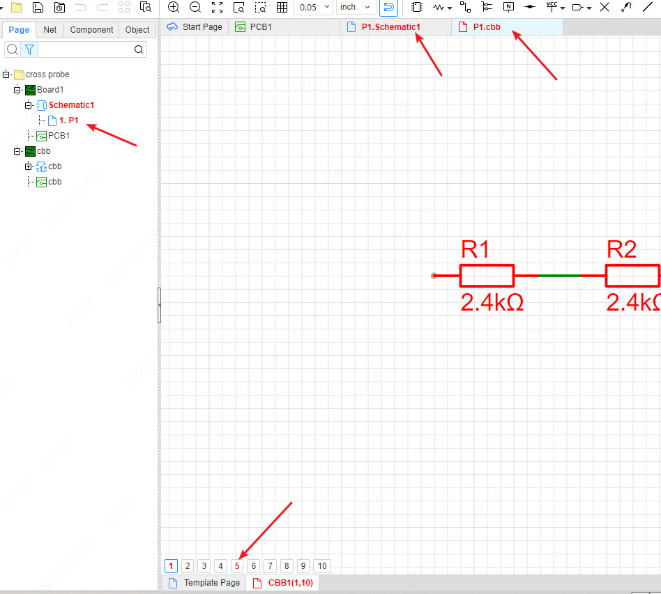
When the principle diagram and PCB open the window separately, you can also use this for cross selection.
If you click on the PCB component directly with the mouse, the element of the schematic window will also be positioned. Use shortcut keys for cross selection to automatically move the TV to make the component in the center of the canvas.
After the PCB is selected in the component, the cross probe function is selected. According to the unique ID of the component, and select the component of the same ID corresponding to the same ID.
After PCB selected the pad in the component, select the cross -selection function, which will highlight and select the pins of the same number of the corresponding components in the original Plains.
The filter panel is checked in the net in the PCB. At the same time, after selecting a net in the canvas, the corresponding net will be highlighted and selected. If there are multiple pages at the same time, the net will be opened at the same time, and these pages will be opened at the same time and switch to switchTo the first page.